Researchers from the Department of Physics at the University of Warsaw, working with teams from the Łódź University of Technology, the Warsaw University of Technology, and the Polish Academy of Sciences, have created a structure that can capture infrared light with a layer of only 40 nanometers. Their method is based on a design known as a “subwavelength grating” made of a special material called molybdenum diselenide (MoSe).2). The findings are reported in the journal ACS Nano.
Controlling light on a very small scale is the key to advancing modern technology. As traditional electronics begin to reach their limits, photonics offers an alternative by using light instead of electrons to transport information. Because photons travel so fast and have no mass like electrons, light-based devices can be even faster, opening the door to more powerful and efficient technologies.
The Light Wavelength Challenge
Light behaves like a particle and a wave, and this wave nature creates an edge. Each type of light has a wavelength, which determines how small a building can be while controlling it effectively. Visible light has wavelengths of several hundred nanometers, while infrared light reaches a micrometer or more. This raises an important question: can light be confined to structures smaller than its wavelength?
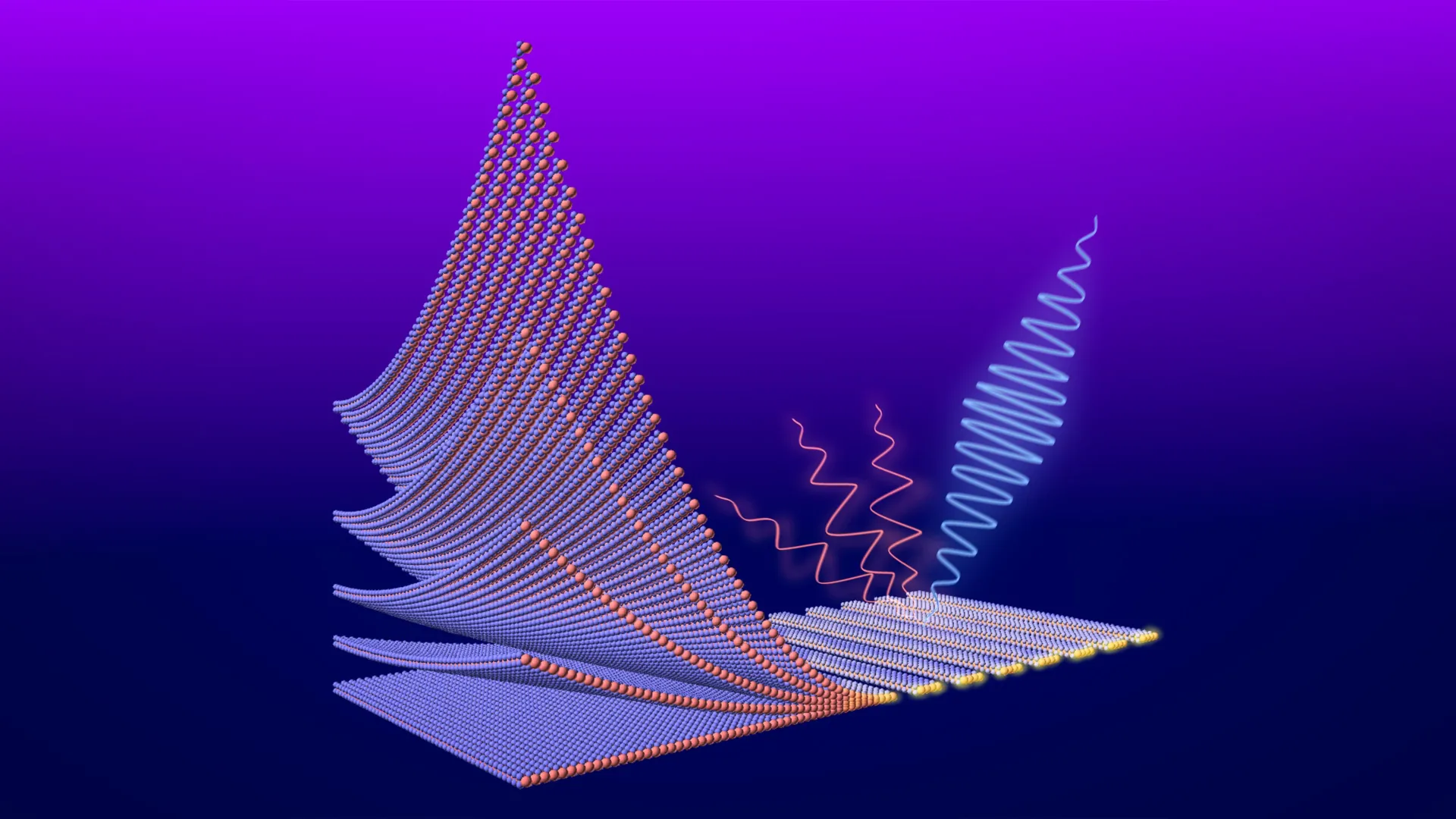
A team of researchers has shown that this is indeed possible. By engineering a subwavelength grating, they were able to trap infrared light in a layer just 40 nanometers thick. This structure consists of parallel, spaced fibers that interact with light in a prism-like manner. When these fibers are placed closer together than the wavelength of light, the grating can act as a close-up mirror while trapping the light in a very small volume.
Why Does Molybdenum Diselenide Work Well?
Earlier versions of such gratings, made of materials such as silicon or gallium compounds, required a thickness of several hundred nanometers to work effectively. Reducing their size has caused them to lose their ability to block light. The main difference of this new method is the use of molybdenum diselenide, which has a very high refractive index. Simply put, light slows down in this material more than in others. While light is delayed about 1.5 times in glass and about 3.5 times in silicon or gallium arsenide, it is 4.5 times slower in MoSe.2. This powerful retardation effect causes the structure to be dramatically reduced while effectively trapping light, resulting in a layer that is more than a thousand times thinner than a human hair.
Converting Infrared Light to Blue Light
MoSe2 it also brings additional benefits. Like graphene, it forms layered structures, but unlike graphene, it is a semiconductor. It also exhibits unusual optical behavior, including a process known as third harmonic generation. In this process, three infrared photons are combined into one high-frequency photon, effectively converting the infrared light into visible blue light. Because the grating focuses so much infrared light, this switch is very efficient. The researchers found that the effect is 1,500 times stronger compared to a flat layer of the same material.
Another major advance is in how that information is created. In the past, thin layers of MoSe2 they are made using exfoliation — a process similar to peeling off layers from a crystal with sticky tape. Although simple, this method is inconsistent and limited to very small areas, usually around ten micrometers, which are not suitable for real-world applications.
To overcome this, the team used molecular beam epitaxy (MBE), a well-designed method of growing semiconductor layers. This method allowed them to produce large, uniform MoSe2 films that are many square inches long. Despite this large size, the membrane maintained a thickness of only 40 nanometers, which made it extremely dimensional. In comparison, the ratio of thickness and size of this scale is about one million to one million, while the standard A4 paper has a ratio close to 1:2000.
About Active Photonic Devices
These results suggest that molybdenum diselenide produced in this way could significantly change the way light is controlled in future technologies. Buildings no longer need to be dense to control light effectively. Instead, very thin enemies can do the same job, and in some cases even better. Because the manufacturing process is scalable, the path to real-world applications, such as photonic integrated circuits, is becoming more realistic.
Funding and Support
The research was funded by the National Science Foundation under the projects OPUS 2020/39/B/ST7/03502 and 2021/41/B/ST3/04183, with the funds of the European Union under the grant ERC-ADVANCED No. Warsaw under Good Design – Research University (IDUB) New Ideas for Important Research Areas II No. 501-D111-20-2004310 entitled “Ultrathin subwavelength gratings based on dichalcogenides.”
#Scientists #trap #light #area #times #thinner #hair